Another advantage of digital electronics is the ability to express signals in terms of logic equations using standard terms from logic: and, or, and not. These functions can be represented by truth tables as shown below with A and B as inputs and C as output.
| and | or | not | |||||||
| A | B | C | A | B | C | A | C | ||
| 0 | 0 | 0 | 0 | 0 | 0 | 0 | 1 | ||
| 0 | 1 | 0 | 0 | 1 | 1 | 1 | 0 | ||
| 1 | 0 | 0 | 1 | 0 | 1 | ||||
| 1 | 1 | 1 | 1 | 1 | 1 | ||||
These logic functions can be represented using a shorthand notation, and is represented by . or &, or is represented by + or #, and not is represented by ~ or ! (there are also other conventions, the most common is to put a bar over the variable). Thus the equation D equals A and B or not C can be represented as
D = A . B+ ˜C or by D = A & B # !C
Obviously this equation has different meanings depending on whether the and or the or function is performed first and parentheses can be used in the normal way to get rid of the ambiguity
D = (A . B)+ ˜C
Other functions that are common are nand and nor. The nand function is an and function followed by a not, nor is an or function followed by not. The symbols used in schematics for these functions are given below:

Logic equations, like any other, can get complicated quickly. To simplify logic equations a system called Boolean algebra (after the mathematician George Boole) was developed. A short selection of its theorems is listed.
| (1) A.0 = 0 | (6) A+1 = 1 | !A.!B | (11) (A.B).C = A.(B.C) |
| (2) A.1 = A | (7) A+Ã = 1 | 1 | (12) A.(B+C) = A.B+B.C |
| (3) A.Ã = 0 | (8) A+A = A | 0 | (13) A+(B.C)= (A+B).(A+C) |
| (4) A+0 = A | (9) A+B = B+A | 0 | (14) !(A+B) = !A.!B |
| (5) A.A = A | (10) (A+B)+C = A+(B+C) | 0 | (15) !(A.B) = !A+!B |
Some of these rules are quite obvious. For example if we make out the truth table for rule (1) we get:
| A | A.0 |
| 0 | 0 |
| 1 | 0 |
Some of the other rules are not so obvious. For example rule 14 yields the truth table shown below
| A | B | !A | !B | A+B | !(A+B) | !A.!B | |
| 0 | 0 | 1 | 1 | 0 | 1 | 1 | |
| 0 | 1 | 1 | 0 | 1 | 0 | 0 | |
| 1 | 0 | 0 | 1 | 1 | 0 | 0 | |
| 1 | 1 | 0 | 0 | 1 | 0 | 0 |
The truth table shows that rule 14, !(A+B) = !A.!B, is correct.
These theorems can be used to simplify equations. For
example if we start off with the expression
D = (A.B+(A+C.˜C)).A+B,
we can apply the rules in turn to simplify it.
D = (A.B+(A+C.˜C)).A+B apply 3 D = (A.B+A).A+B apply 2 D = (A.B+A.1).A+B apply 12 D = (A.(B+1)).A+B apply 6 D = A.A+B apply 5 D = A+B
As with the algebra you learned in elementary school, this kind of simplification gets tedious, and messy, quickly. Luckily there is a graphical shortcut to doing logic minimizations called a Karnaugh map. This introduction will only cover Karnaugh maps with up to four variables, though the technique can be generalized to larger systems - though these systems are usually simplified using computers. Consider the truth table of the equation given above, which is given in the forma of a truth table and a three variable Karnaugh map:

One way to get a solution is simply to write an expression for each true result in the table. For example, the lower-leftmost true result from the Karnaugh map represents the case where A=1 and B=0 and C=0 and it can be written as A.˜B.˜C. The true result next to it can be written as A.˜B.C. Now to develop a logic expression, we would just or together all of these terms. Thus our result (including an expression for each true term -- 6 in all) is:
A.˜B.˜C + A.˜B.C + A.B.C + A.B.~C + ˜A.B.C + A.B.˜C
This is called the sum-of-products form. Although this expression is correct, it is also unwieldy. We could use the theorems of Boolean algebra to simplify the expression, which is often difficult and does not guarantee a best solution. However we can use a visual technique based on Karnaugh maps to develop a minimal sum-of-products solution.
To get the simplified equation one takes the table and encircles as many 1's as possible in rectangular groups that have 1, 2, 4, or 8 elements (i.e., any power of 2). The idea is to make the groupings as large as possible. For the example above this can be accomplished with 2 groupings:

If you examine these groupings carefully you can see that the red grouping has no dependence on the variables A or C, and is totally described by the statement B=1. The blue group on the other hand has no dependence on B or C and is described by the statement A=1. Therefore to include the elements from both groups we can use the equation A+B. If you had used smaller groups you would have obtained an equivalent, though more complicated, expression. Try it. This graphical method is clearly easier than the technique used earlier that employed algebraic simplifications.
You should examine the map shown above and convince yourself that any grouping of a single element needs all three variables to describe it. For instance the uppermost "1" on the right hand side is described by B.˜C. Ã A grouping of two gets rid of the dependence on one of the variables (the two rightmost ones have no dependence on A and are given by B.˜C). A group of four, as you have seen, depends only on one variable. Therefore by choosing the smallest number of groups (i.e., the largest groups), you will come up with the minimal equation describing those groups. The result obtained with the Karnaugh map is called the minimal sum of products form because it generates the smallest number of product (anded) terms.
Also, if you look at the table again you can convince yourself that it is possible to "wrap-around" the ends of the table, as shown

The two groups are represented by B.C (the red group) and the blue group that wraps around by A.˜C.
This technique also works for two variables (trivial), four variables (shown below), and even more (though this gets complicated and will not be described here). A typical four variable map and its groupings are shown here.

which simplifies to: A.B.D.˜C + Ã.B.˜D + Ã.C + ˜B.C. Prove it to yourself.
Months in school
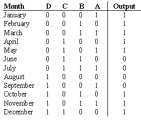
Truth Table and Karnaugh map

Alternate solution (others possible)


